Company News

A research team from Xi'an Jiaotong University has successfully prepared a (111) surface heteroepitaxial single crystal diamond substrate
GaN, as a typical representative of third-generation semiconductor materials, has advantages in key properties such as bandgap width, breakdown field strength, electron mobility, thermal conductivity, and maximum operating temperature. GaN power devices have high conversion efficiency, low conduction loss, high operating frequency, large bandwidth, and high power density, and have been widely used in communication, radar, satellite, power electronics, and other fields. As devices develop towards smaller sizes, higher power, and higher frequencies, the size of the device junction region decreases and the heat flux density increases significantly, resulting in a sharp rise in junction temperature, which severely limits the further improvement of power density and may even lead to device burnout, manifested as a significant decrease in power density when MMICs and PAs are outputting high power. Using diamond material with ultra-high thermal conductivity as a heat sink can effectively improve the self heating effect of GaN based high-power electronic devices. However, bonding technology inevitably generates an amorphous intermediate layer with high thermal resistance at the interface between the two wafers, which affects heat dissipation and cannot fully unleash the enormous potential of diamond in the field of thermal management. The direct epitaxial growth of GaN HEMT structure on (111) plane single crystal diamond using high thermal conductivity AlN superlattice can effectively avoid the generation of high thermal resistance intermediate layer, maximize the heat dissipation ability of diamond, and exponentially improve the device power density. Therefore, the development of large-area, high-quality single crystal (111) diamond substrates is urgently needed.
Professor Wang Hongxing's team at Xi'an Jiaotong University used microwave plasma chemical vapor deposition (MPCVD) technology to achieve epitaxial growth of single crystal diamond (111) on Ir (111)/sapphire surfaces for the first time, and successfully achieved a 20 × 20 mm2 (111) orientation heteroepitaxial single crystal diamond self-supporting substrate. Through SEM, XRD, and EBSD characterization, the half width of the XRD (111) rocking curve is less than 0.6 °, indicating that diamond (111) has excellent single crystal characteristics and has reached the world's leading level.

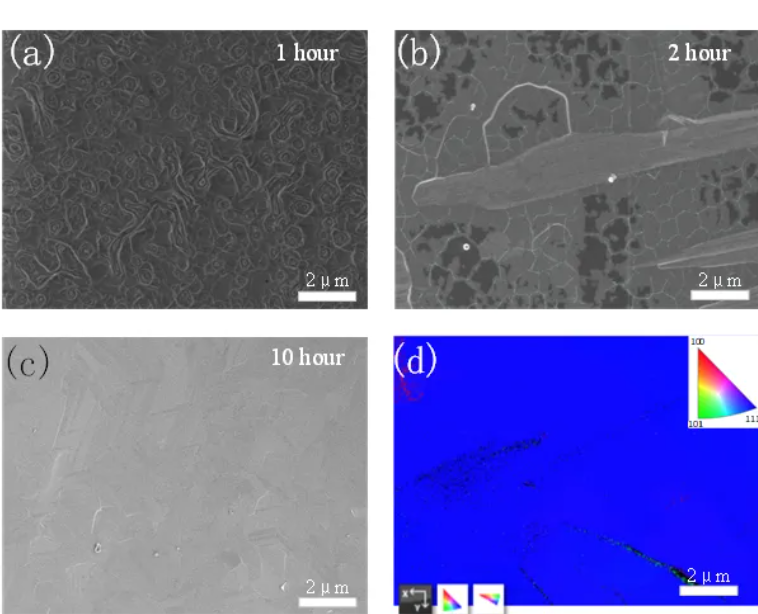
Figure 1 SEM morphology characterization and EBSD characterization of single crystal diamond (111) surface
Figure 1 shows the surface morphology of diamond (111) single crystal thin film on Ir (111)/sapphire surface with epitaxial growth time. In Figure 1 (a), it can be seen that after 1 hour of epitaxial growth, a dense hexagonal structure single crystal diamond (111) continuous thin film is formed. As the epitaxial growth time increases, the surface of the hexagonal structure gradually closes into a continuous and flat thin film, as shown in Figure 1 (b). After 10 hours of epitaxial growth, a flat single crystal diamond (111) surface was formed, as shown in Figure 1 (c). Figure 1 (d) shows the EBSD test pattern of the diamond (111) surface, and the results indicate that the crystal orientation of the diamond (111) surface has good uniformity.

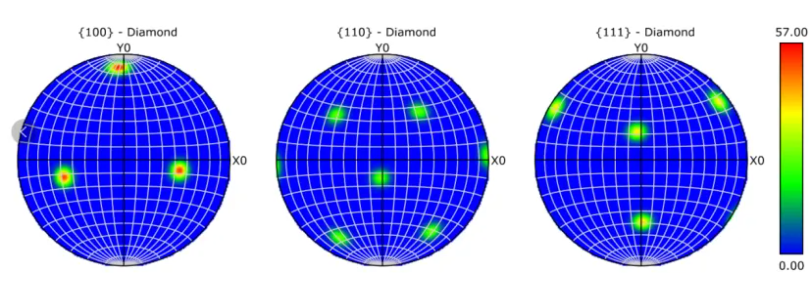
Figure 2 (111) Single crystal diamond pole diagram
Figure 2 shows the polar diagram of the diamond (111) surface, demonstrating that the diamond (111) surface film exhibits excellent single crystal characteristics.

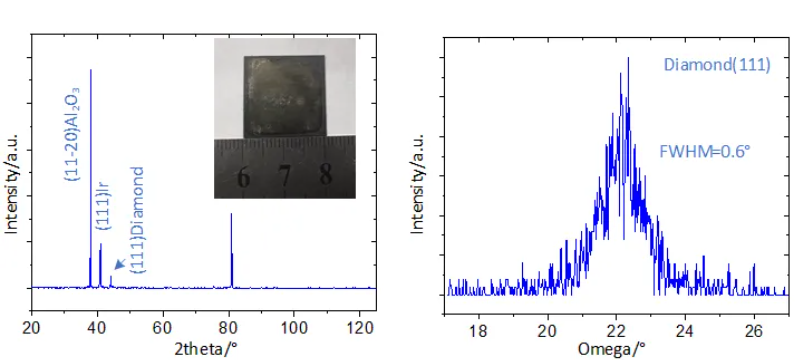
Figure 3 Single crystal diamond XRD curve (a) 20 ° -125 ° 2 θ curve (b) Diamond (111) surface rocking curve
Figure 3 (a) shows the XRD test results of (111) plane single crystal diamond. Within the scanning range of 20-125 °, only alumina substrate, Ir (111), and diamond (111) peaks are present. The illustration shows a self-supporting diamond (111) substrate with a size of 20 × 20 × 0.5 mm2 obtained after long-term growth. Figure 3 (b) shows that the half width at half maximum of the diamond (111) surface rocking curve is 0.6 °, indicating that the diamond (111) surface has good single crystal characteristics.
The Wide Bandgap Semiconductor Materials and Devices Research Center of Xi'an Jiaotong University was established in 2013, and the laboratory director is Professor Wang Hongxing, a nationally appointed expert. After nearly 10 years of development, the laboratory has formed a series of technologies with independent intellectual property rights, including the research and development of diamond semiconductor epitaxial equipment, single crystal/polycrystalline substrate growth, and electronic device development. 48 patents have been authorized, and extensive cooperation has been carried out with domestic large communication companies, China Electronics Technology Group Corporation and other related research institutes on diamond semiconductor materials and devices, promoting the practical development of diamond RF power devices, power electronic devices, MEMS and other devices.